- 您现在的位置:买卖IC网 > Sheet目录1992 > DAC5674IPHPG4 (Texas Instruments)IC DAC 14BIT 400MSPS 48-HTQFP
DAC5674
SLWS148A SEPTEMBER 2003 REVISED OCTOBER 2005
www.ti.com
21
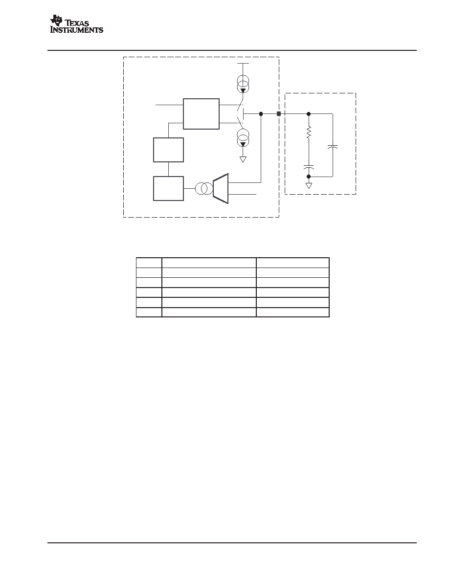
PFD
ref
ICO
Fref
Fvco
LPF
R
C1
C2
DAC5674
External Loop Filter
PN
Figure 22. PLL Functional Block Diagram
Table 5. DAC5674 Evaluation Board PLL Loop Filter Parameters
N(1)
PHASE MARGIN (DEGREES)
BANDWIDTH (MHZ)
2
60
1.6
4
71
1.4
8
77
1
16
78
0.7
32
74
0.4
(1) N is the VCO divide-down factor from prescale and interpolation.
Non-Harmonic Clock-Related Spurious Signals
In interpolating DACs, imperfect isolation between the digital and DAC clock circuits generates spurious signals
at frequencies related to the DAC clock rate. The digital interpolation filters in these DACs run at subharmonic
frequencies of the output rate clock, where these frequencies are fDAC/2 , N = 1,2. For example, for 2×
interpolation only one interpolation filter runs at fDAC/2; for 4× interpolation, on the other hand, two interpolation
filters run at fDAC/2 and fDAC/4. These lower-speed clocks for the interpolation filter mix with the DAC clock
circuit and create spurious images of the wanted signal and second Nyquist-zone image at offsets of fDAC/2N.
Figure 23 shows the location of the largest spurious signals for 4
× interpolation for a real signal. With a real
output signal, there is no distinction between negative and positive frequencies, and therefore the signals that
appear at negative frequencies wrap and potentially fall near the wanted signal. In particular, at IFs near fDAC/8,
fDAC/4, and fDAC × 3/4 (50 MHz, 100 MHz, and 150 MHz in this example), the mixing effect results in spurious
signals falling near the wanted signal, which may present a problem depending on the system application. For
a frequency-symmetric signal (such as a single WCDMA or CDMA carrier), operating at exactly fDAC/8, fDAC/4
and fDAC × 3/4, the spurious signal falls completely inside the wanted signal, which produces a clean spectrum
but may result in degradation of the signal quality.
发布紧急采购,3分钟左右您将得到回复。
相关PDF资料
DAC7621EBG4
IC SNGL 12BIT PARALLEL D/A 20SSO
DAC7801KPG4
IC DUAL 12BIT CMOS DAC 24-DIP
DAC8043AESZ
IC DAC 12BIT MULT SRL INP 8SOIC
DAC8043GP
IC DAC 12BIT MULTIPLY CMOS 8-DIP
DAC8221GP
IC DAC 12BIT DUAL W/BUFF 24-DIP
DAC8222GPZ
IC DAC 12BIT DUAL W/BUFF 24DIP
DAC8229FSZ-REEL
IC DAC 8BIT DUAL V-OUT 20SOIC
DAC8248FS
IC DAC 12BIT DUAL W/BUFF 24-SOIC
相关代理商/技术参数
DAC5674IPHP-ND
制造商: 功能描述: 制造商:undefined 功能描述:
DAC5674IPHPR
功能描述:数模转换器- DAC 14-Bit 400 CommsDAC RoHS:否 制造商:Texas Instruments 转换器数量:1 DAC 输出端数量:1 转换速率:2 MSPs 分辨率:16 bit 接口类型:QSPI, SPI, Serial (3-Wire, Microwire) 稳定时间:1 us 最大工作温度:+ 85 C 安装风格:SMD/SMT 封装 / 箱体:SOIC-14 封装:Tube
DAC5674IPHPRG4
功能描述:数模转换器- DAC 14-Bit 400 CommsDAC RoHS:否 制造商:Texas Instruments 转换器数量:1 DAC 输出端数量:1 转换速率:2 MSPs 分辨率:16 bit 接口类型:QSPI, SPI, Serial (3-Wire, Microwire) 稳定时间:1 us 最大工作温度:+ 85 C 安装风格:SMD/SMT 封装 / 箱体:SOIC-14 封装:Tube
DAC5675
制造商:TI 制造商全称:Texas Instruments 功能描述:14-BIT, 400-MSPS DIGITAL-TO-ANALOG CONVERTER
DAC5675A
制造商:TI 制造商全称:Texas Instruments 功能描述:14-Bit, 400MSPS Digital-to-Analog Converter
DAC5675AEVM
功能描述:数据转换 IC 开发工具 DAC5675A Eval Mod RoHS:否 制造商:Texas Instruments 产品:Demonstration Kits 类型:ADC 工具用于评估:ADS130E08 接口类型:SPI 工作电源电压:- 6 V to + 6 V
DAC5675AIPHP
功能描述:数模转换器- DAC 14-Bit 400-MSPS RoHS:否 制造商:Texas Instruments 转换器数量:1 DAC 输出端数量:1 转换速率:2 MSPs 分辨率:16 bit 接口类型:QSPI, SPI, Serial (3-Wire, Microwire) 稳定时间:1 us 最大工作温度:+ 85 C 安装风格:SMD/SMT 封装 / 箱体:SOIC-14 封装:Tube
DAC5675AIPHP
制造商:Texas Instruments 功能描述:IC DAC 14BIT 400MSPS 48-HTQFP